 DLA Lab Suitability
 ITAR
ITAR-
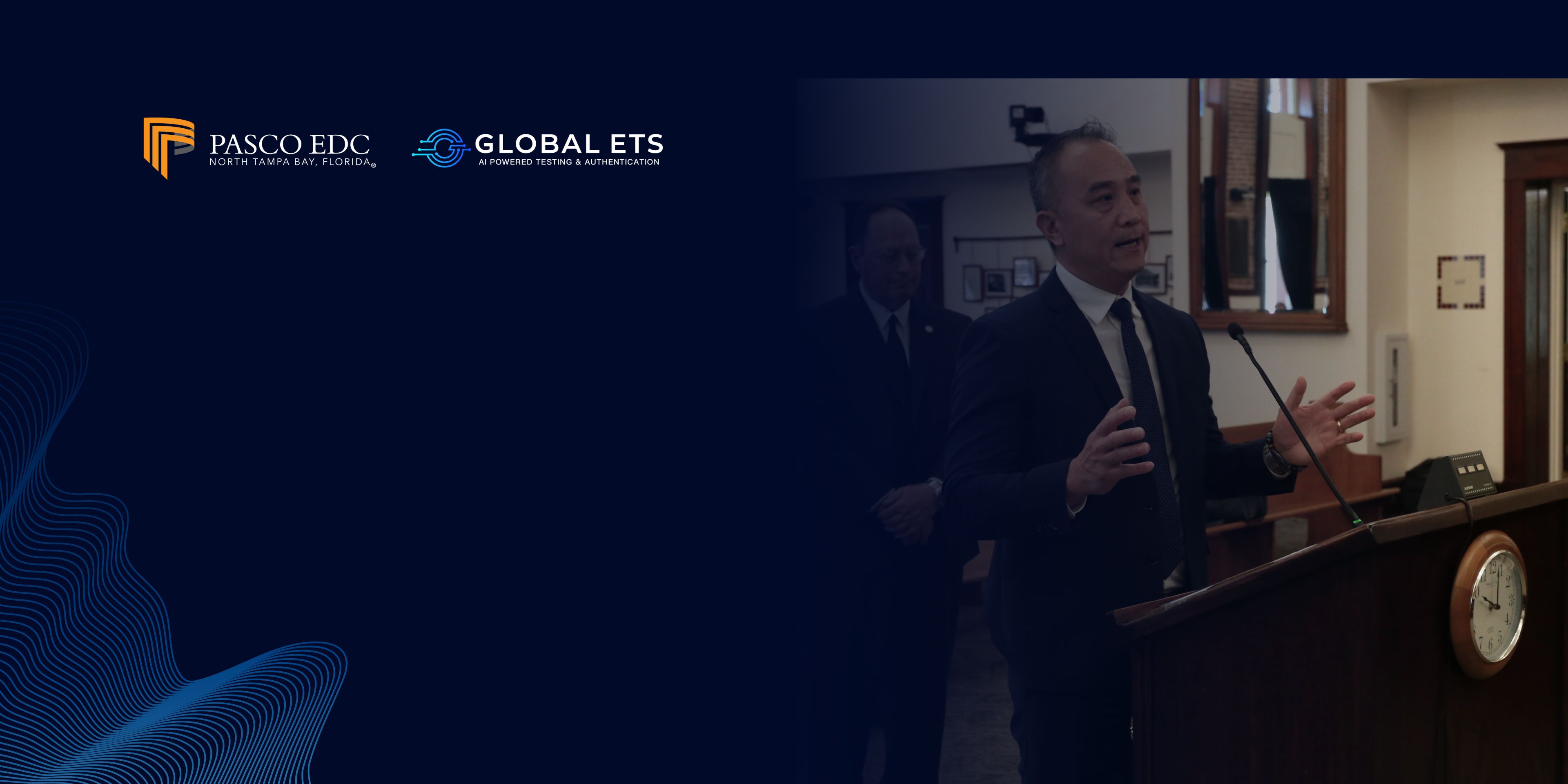
Innovative AI Testing: Global ETS Gets $160k Job Bonus
“As a business owner, feeling supported by the community is crucial, and thanks to Pasco EDC, we’re not just a business here; we’re part of a thriving community committed to mutual growth.”
- Dan Tang, Chief Executive Officer for Global ETS
-
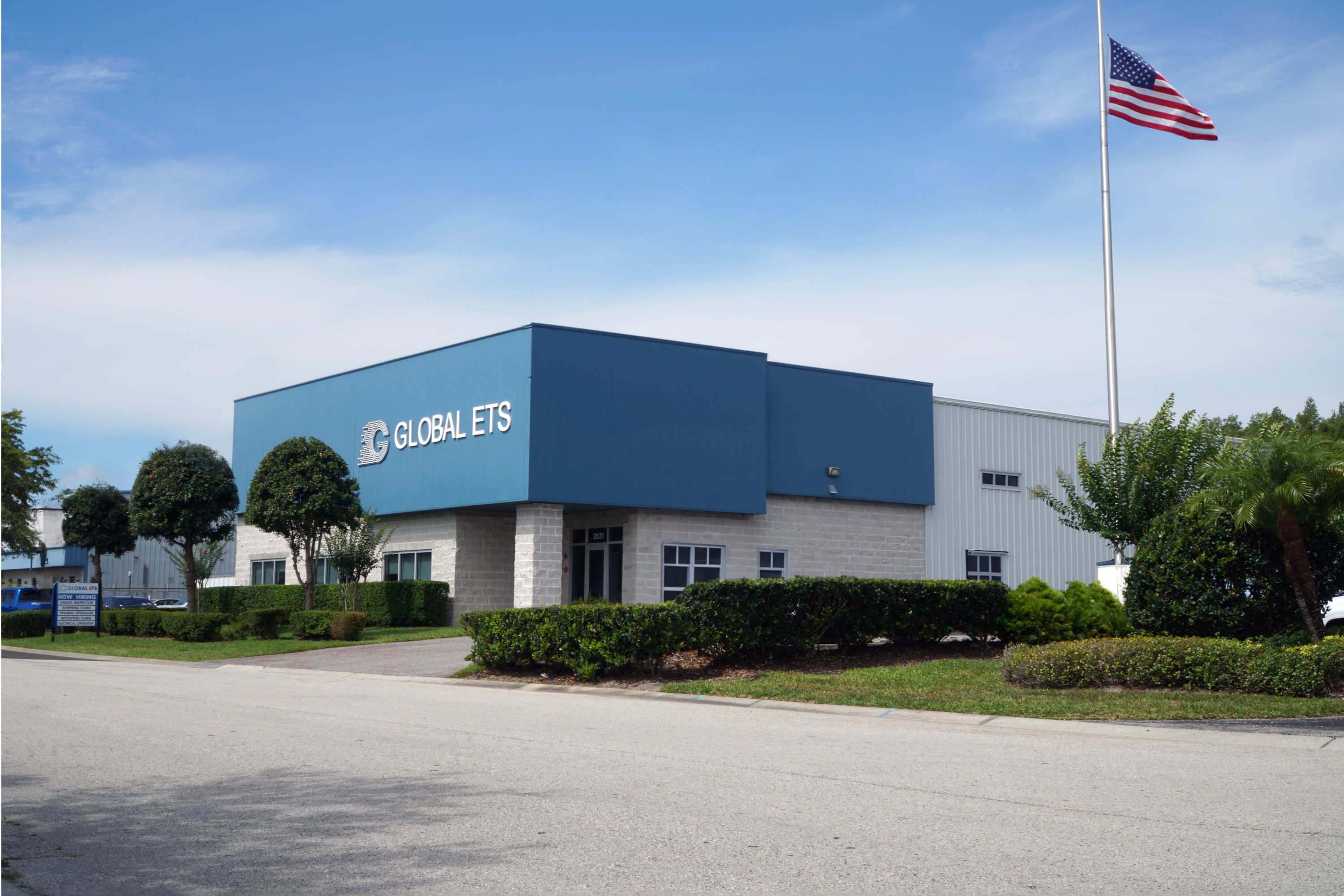
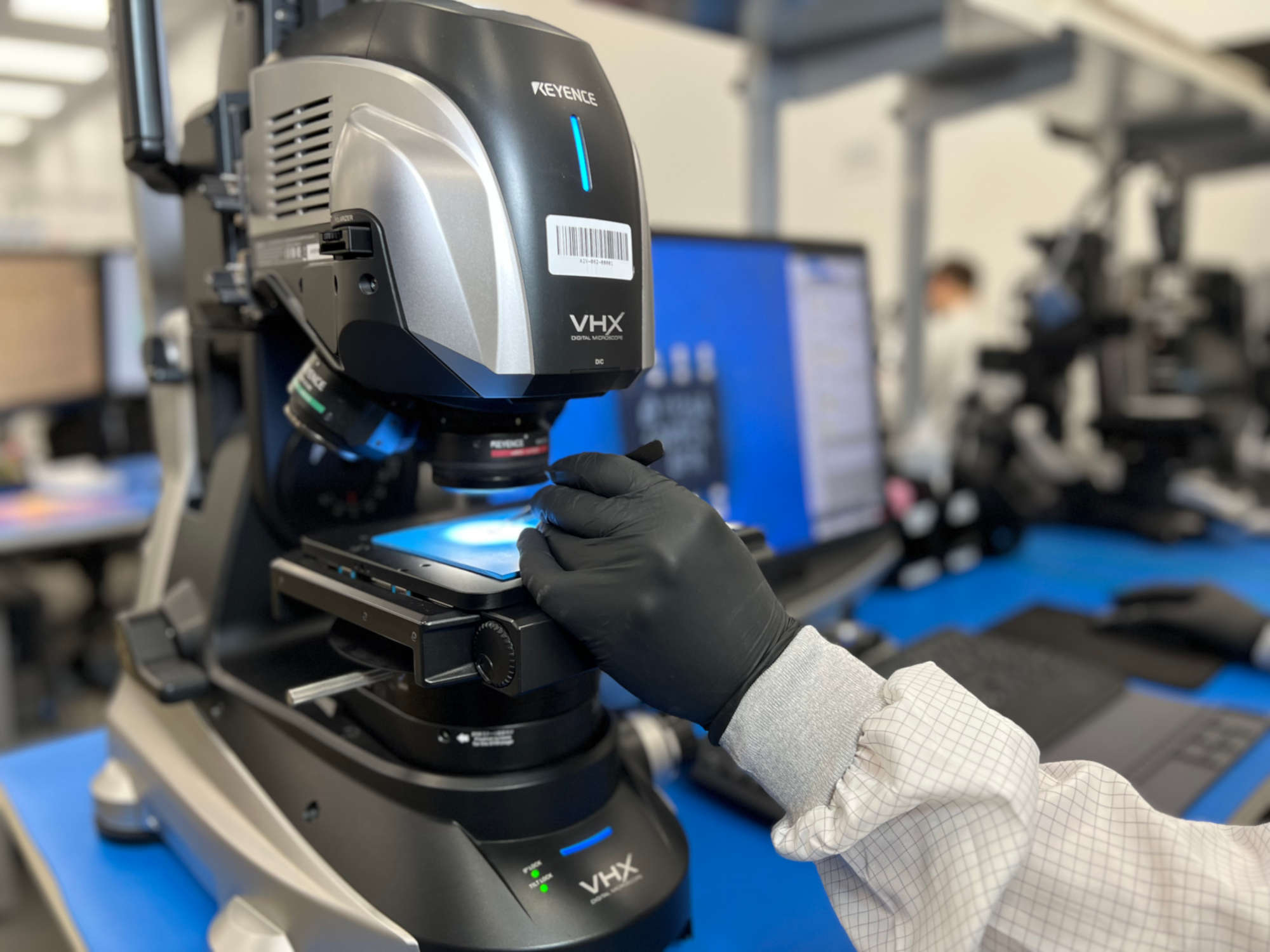
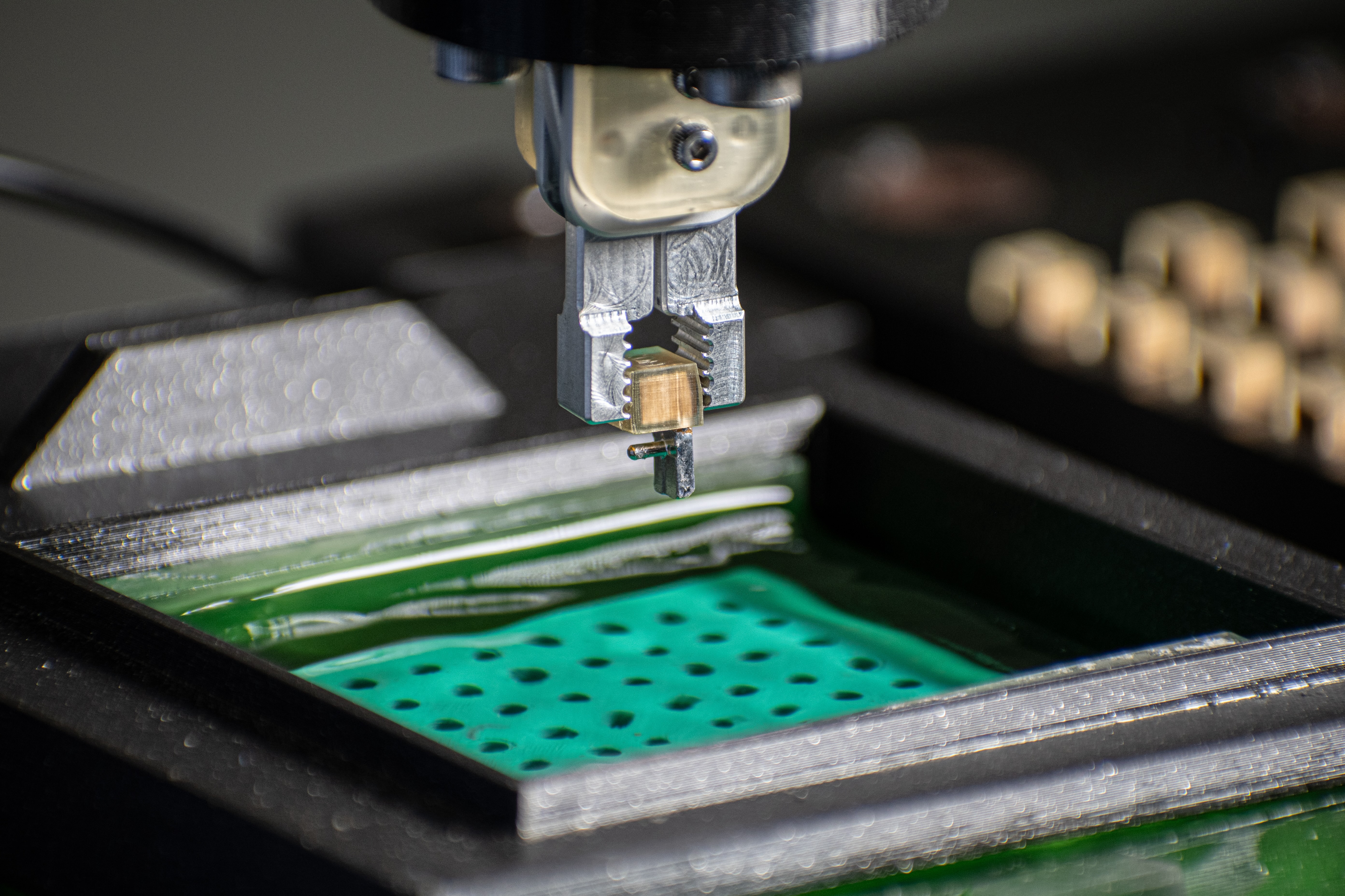
Global ETS: Redefining Electronics Testing Worldwide
Global ETS is the leader in independent electronic component testing and authentication, leveraging a variety of proprietary AI technologies.
Our patented software, hardware, analytical testing, and tracking methods are improving on traditional methods to standardize the component testing process and testing time. At GETS, we tailor solutions to meet your exact specifications, ensuring precision and efficiency. Meeting many test standards such as AS6171, AS9100, and AS6081, GETS is equipped and ready to handle a wide range of authentication needs. Not only is GETS certified for these methods, but we are also an approved laboratory under DLA/QTSL.
Our Services
-
Testing Services
Explore our comprehensive selection of solutions designed to meet all semiconductor needs.Learn More -
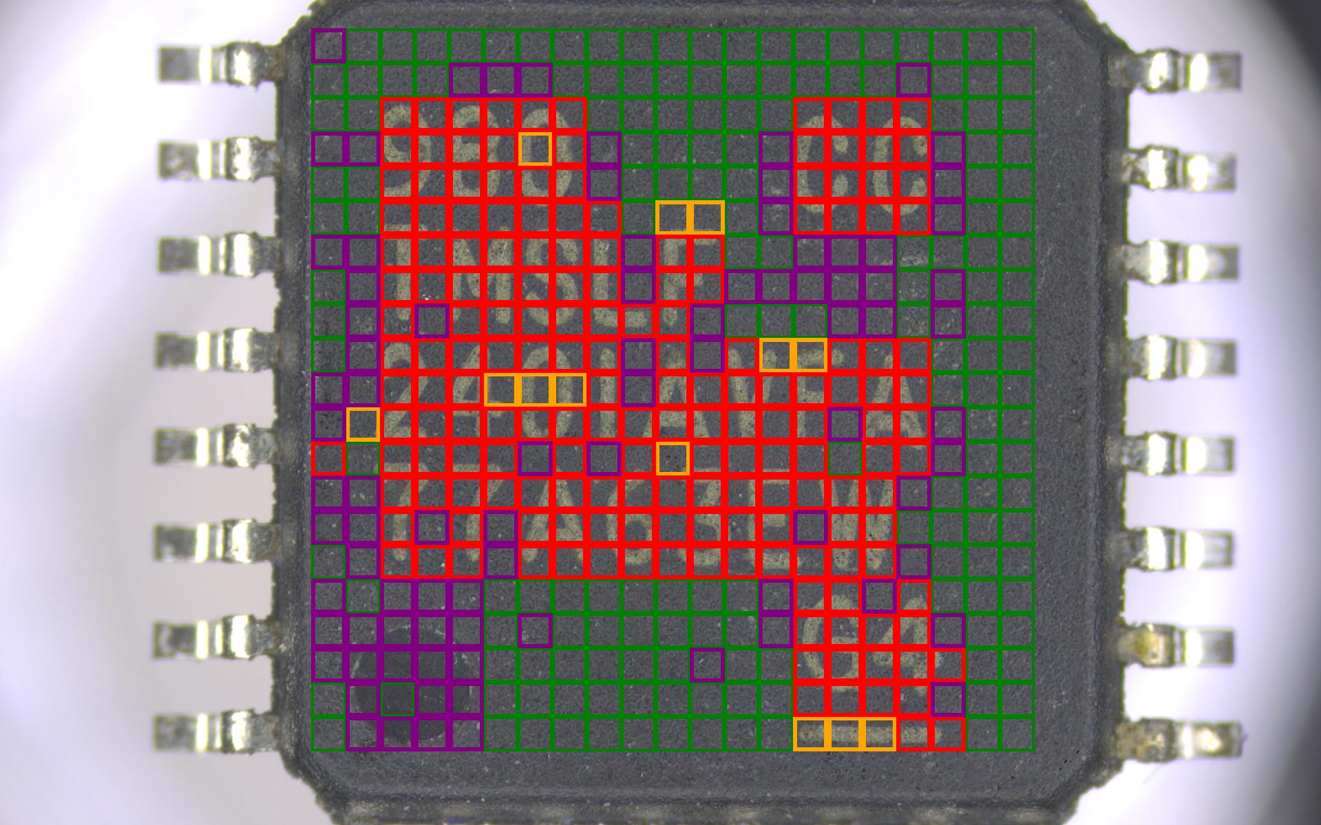
Authentication Scan
Users can now authenticate components seamlessly from any location using this AI-driven system - just by uploading images.Learn More -
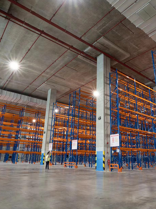
Warehousing & Logistics
Keep your components secure and safe in our brand-new climate-controlled warehouse.Learn More -
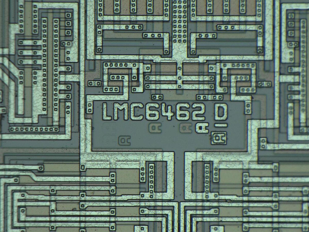
Component Resource Center (CRC)
Our Component Resource Center (CRC) allows for easily accessible part information and die data.Learn More -
Re-Tinning
Renew and enhance the life of your semiconductor components with our re-tinning and re-balling services.Learn More
We are strategically located throughout the world.
View More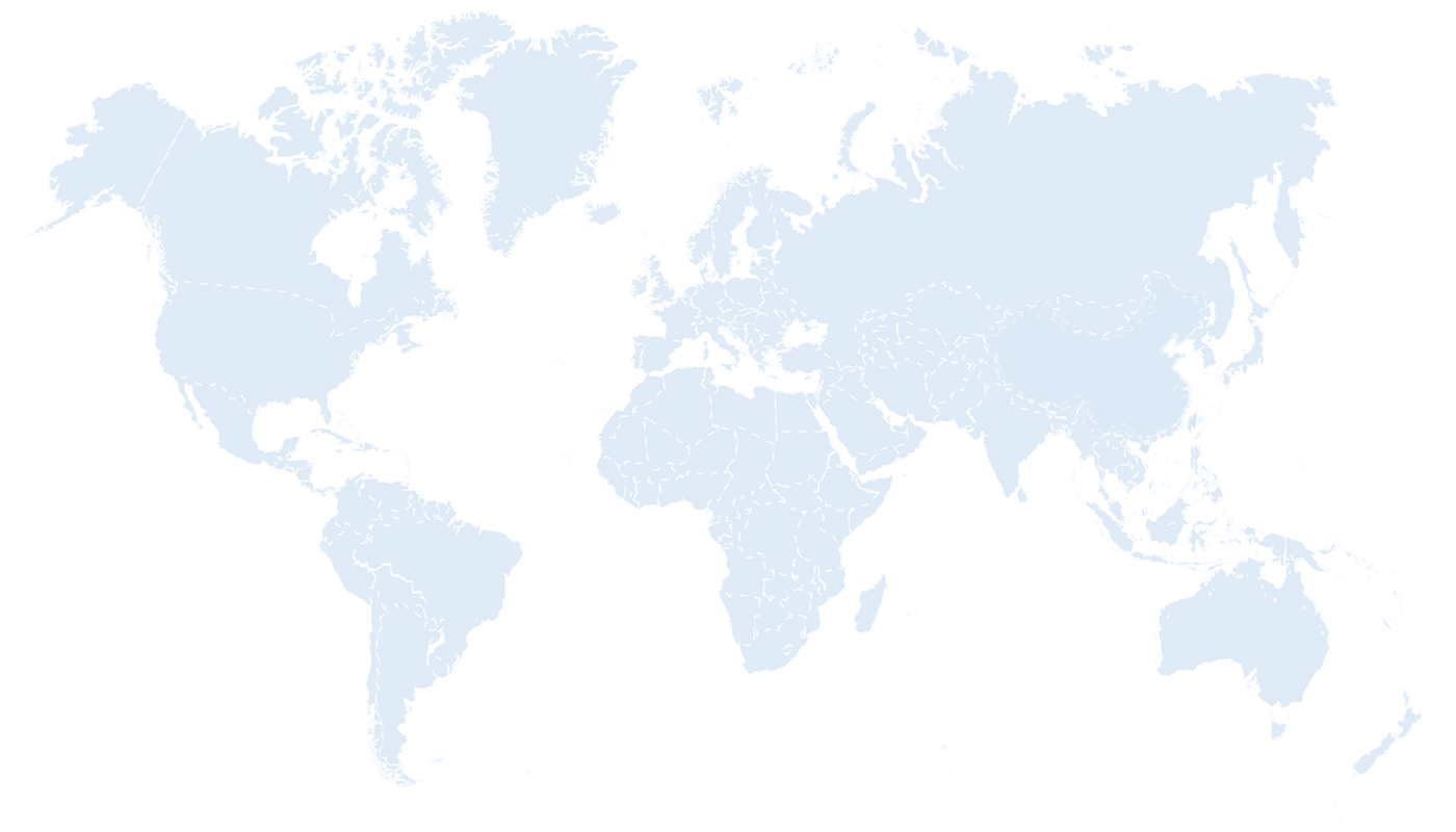
Florida
Malaysia
California
Shenzhen
Netherlands
Hong Kong
Taiwan
Level 3
Level 2
Level 1
Insights
-
April 1, 2024
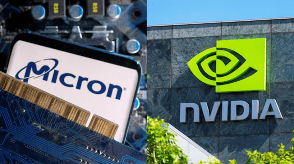
AI's Role in Filling the Market Gap
Micron's FYQ2 financial report, released on March 20, showed exceptional performance ...View More -
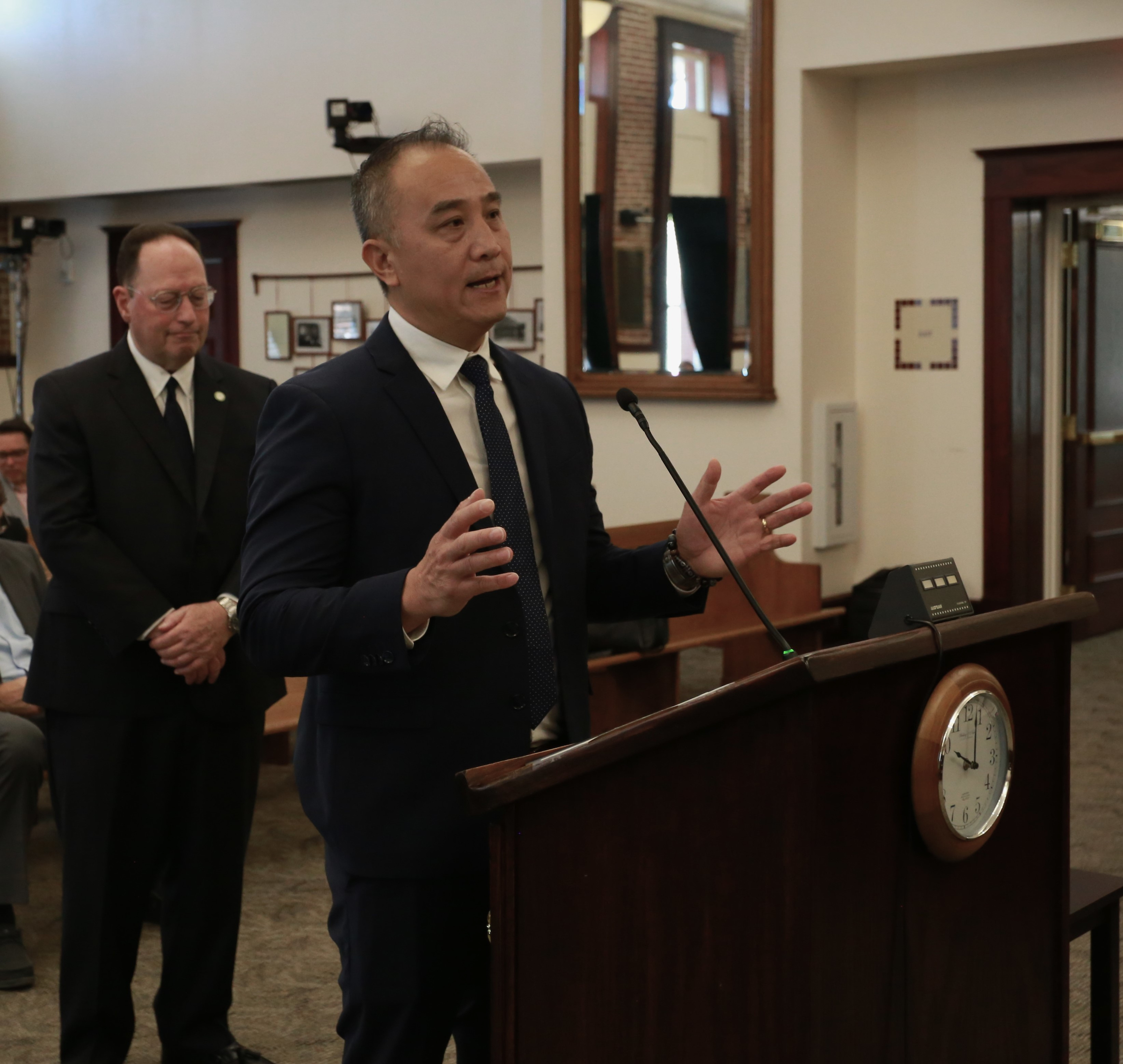
March 13, 2024
High-tech Pasco company earns $160,000 job creation bonus
Over the last two years, international microchip-testing company Global ETS ...View More -

Jan 26, 2024
Who is the rock-solid existence?
Major semiconductor companies, including Texas Instruments, Intel, and STMicroelectronics ...View More