 DLA Lab Suitability
 ITAR
ITARComponent Testing Services
General Testing Services
Advanced Services
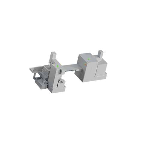
Incoming Inspection
Incoming Inspection
The incoming inspection is performed upon receiving parts. This process is crucial, as it involves the documentation of what was received in. Verifying part numbers, purchase orders, and part count are performed during this inspection.
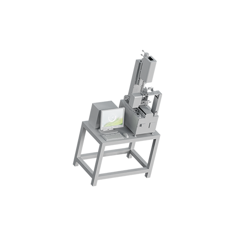
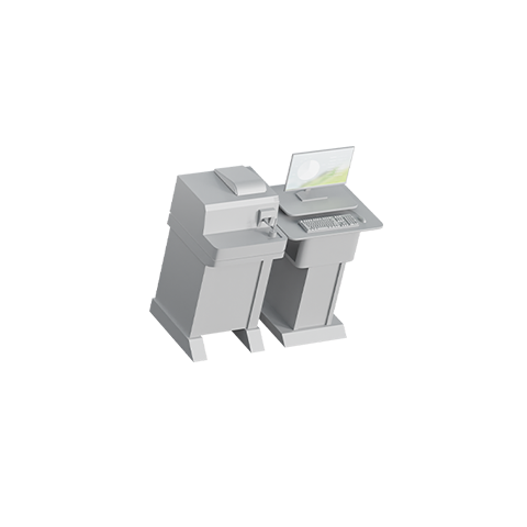
External Visual Inspection
External Visual Inspection
The detailed visual inspection is a thorough examination of parts, using 40x magnification. This process can detect discrepancies with the devices against the testing standard, as well as customer requirements.
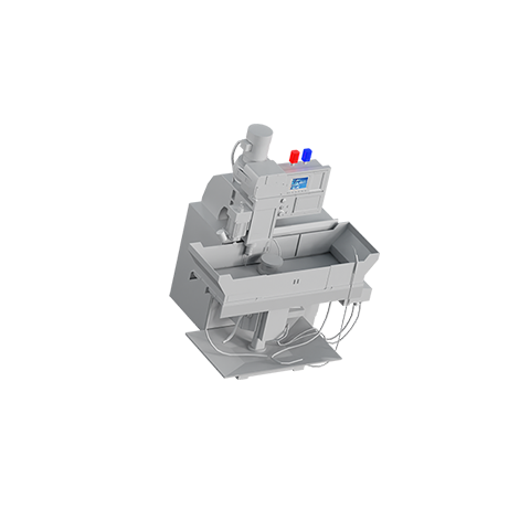
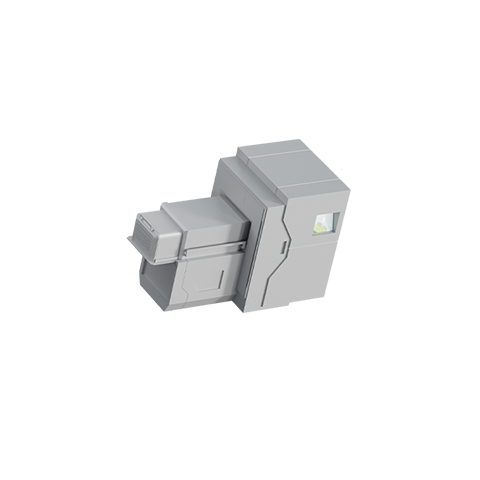
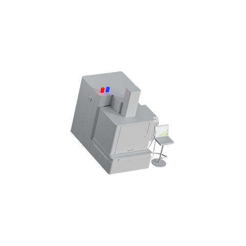
X-Ray / XRF
X-Ray / XRF
XRF Testing: XRF (X-ray Fluorescence) is a non-destructive test used on electronic parts to analyze their material composition.
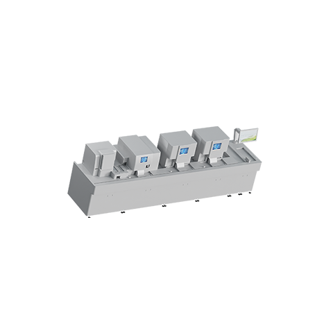
Electrical Testing
Electrical Testing
Passive component testing involves a comprehensive array of methods and measurements designed for the assessment and characterization of passive electronic components, including resistors, capacitors, and inductors. These components, in contrast to their active counterparts, do not amplify or switch electronic signals. This underscores the critical importance of utilizing highly accurate testing equipment.
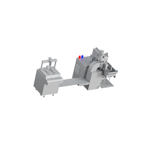
Chemical & Destructive Test
Chemical & Destructive Test
The chemical & destructive tests are used to verify the attributes of a component and ensure they meet required standards.
Shipping
Shipping
As the final step in the authentication process, it is crucial for ensuring the traceability and protection of components. Many components tested here at GETS are used in critical industries, including the defense and medical sectors.
.png)
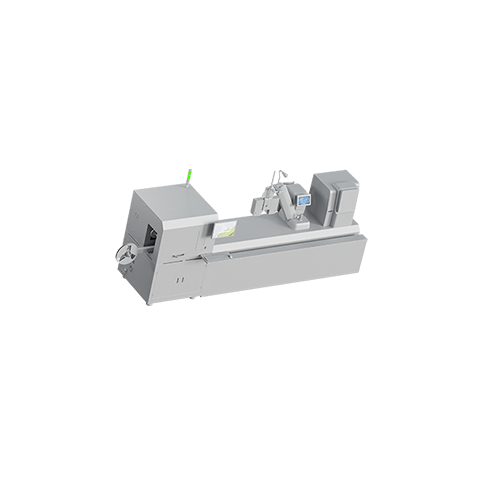
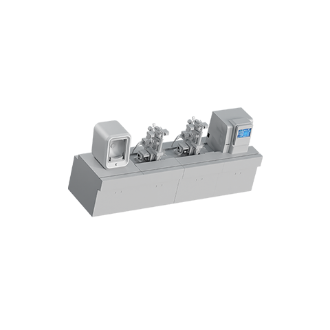
Tape & Reel
Tape & Reel
The Tape & Reel process is a standard process when dealing with electronic components, and involves preparing and packaging parts for later use.
Baking
Baking
Baking after testing is typically done to eliminate any residual moisture that may have been absorbed during the testing process. This helps ensure the reliability and performance of the electronic components, especially in moisture-sensitive applications where even small amounts of moisture can have adverse effects.
Material Analysis
Material Analysis
Material analysis tests are necessary to evaluate composition, structure, and properties of part materials. Equipped with the newest tchnologies, GETS is able to complete an array of advanced material analysis tests.
Re-Tinning
Re-Tinning
The tinning procedure is used for a variety of purposes, such as the refurbishing of “Legacy Components”, tin whisker mitigation, and conversion of SN/Pb components to RoHS and vice versa.
Reballing
Reballing
Reballing is used to replace the solder balls on a specific component, typically BGA’s (Ball Grid Array). When the existing solder balls on a component are damaged or degraded, replacing them on parts that would otherwise be discarded saves cost and reduces electronic waste in the industry.
Programing Services
Programing Services
Our programming service offers electronics manufacturers the opportunity to subcontract the programming of their components. This alleviates the intricacies and extensive time commitments associated with programming during testing, leading to increased production line efficiency and cost-effectiveness.
Die Level Testing
Die Level Testing
Die level testing means examination of individual semiconductor dies to verify that they meet required specifications and standards. The goal is to identify and address issues at the die level to prevent them from affecting the overall performance and reliability of the final electronic components or systems.
Firmware Security Analysis
Firmware Security Analysis
Firmware security analysis encompasses many different solutions, but the main focus is to ensure the security of software embedded within electronic devices. Potential vulnerabilities, exploits, and weaknesses may be found while conducting analysis.
Other
Other
This paragraph is a substitute copy This paragraph is a substitute copy